|
Capabilities
-
Determination of semiconductor gap by photoreflectance
In this technique, the sample is scanned with photons of different energies while the reflectance of the sample is monitored. When the energy of the photon matches the gap of the semiconductor, the reflectivity of the sample peaks what allows to measure the gap. Requirements: sample size less than 1cm Ø; sample thickness less than 10 mm; measurement range 400 to 2500 nm.
- Characterization of the quantum efficiency of novel solar cells
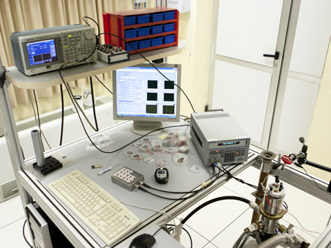
This technique consists of illuminating the solar cell with photons of different energies while monitoring the electric current produced by the solar cell in short circuit conditions. The measurement allows to determine the percentage of photons of a given energy that are effectively converted into electric current. Requirements: sample size less than 4 cm x 4 cm; sample thickness less than 5 mm; measurement range 400 to 1700 nm; samples must be provided with wired contacts.
- Capability to obtain the current-voltage characteristics of solar cells in dark and in illumination conditions
This technique consists of biasing the solar cell with a given voltage and measure the electric current circulating. The experiment can be done without illumination and under illumination. Requirements: sample size less than 1 cm x 1 cm; sample thickness less than 5 mm; measurement range 100nA to 1 A; samples must be provided with wired contacts.
- Capability to obtain the current-voltage characteristics up to light concentrations of 2500x
Under optimal conditions, it is possible to illuminate the solar cell with a light intensity up to 2500 times the light that comes from the sun using flash light pulses. Requirements: sample size less than 1 cm x 1 cm; sample thickness less than 5 mm; measurement range 100nA to 1 A; samples must be provided with wired contacts.
- Performance of FTIR tests in order to determine the optical absorption coefficient of photovoltaic materials mainly in the infrared
The FTIR technique (Fourier Transform in the Infrared) consists in illuminating the sample with photons with energy in the infrared while superposing the incident photon beam with the photon beam that is transmitted by the sample. When the sample is displaced the interference pattern between both beams changes what allows to measure the absorptivity of the sample in the infrared. Requirements: sample size larger than 1 cm x 1 cm; sample thickness less than 5 mm; measurement range 800nm to 2000 nm.
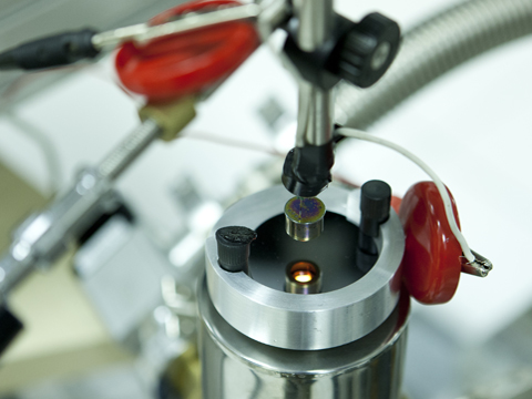
- Undertaking of DLTS measurements to study semiconductor defects
The DLTS (Deep Level Transient Spectroscopy) technique consists in applying a voltage pulse to the sample while measuring its capacitance. By measuring how fast or slow this capacitance evolves with time in response to the pulse it is possible to determine how effective defects in a semiconductor are for capturing electron-hole pairs. Requirements: sample size less than 1 cm Ø; sample thickness less than 5 mm; measurement range 77 K to 330 K; samples must be provided with wired contacts.
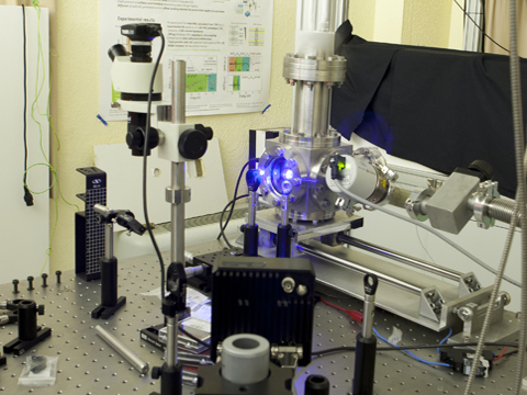
- Measurement of photoluminescence and electroluminescence of materials and solar cells
In a photoluminescence experiment the sample is excited with a laser beam and in a electroluminescence experiment the sample is excited with electric current. In both cases, the number of photons emitted by the sample under test as well as their energy is measured what allows to gather information of the quality of the sample and the energy of its gap. Requirements: sample size larger than 0.5 cm x 0.5 cm; sample thickness less than 5 mm; measurement range 400nm to 2000 nm.
- Capability to determine roughness of the semiconductor surface*
The roughness of a the sample is measured with an instrument call profilometer. In this technique the vertical displacement of a probe is measured while it scans the surface of the sample. Requirements: sample size less than 10 cm Ø; sample thickness less than 30 mm; measurement range 77 K to 330 K; non-deformable material.
- Low temperature measurements
Quantum efficiency and current-voltage characteristic measurements can be carried out at cryogenic temperatures typically as low as 10 K. Sample size less than 1x1 cm; sample thickness less than 1 mm; samples must be contacted with 2 wires; encapsulation provided must be heat dissipating and not break at low temperatures.
(*) Under ISO9001 STANDARD
|
|
 |