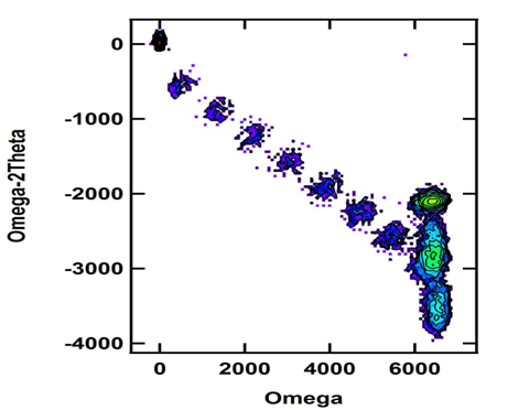
- High Resolution X-Ray Diffraction: an X-Pert Panalytical diffractometer is used. HRXRD analysis meets many of the analytical needs of crystal science. Typical scans obtained in our laboratory are Rocking Curves, Coupled Scans and Reciprocal Space Maps, which reveal the layers parameters such as ternary composition, d-spacing, mismatch or stress.
- Doping profile of semiconductor materials by Electrochemichal Capacitance-Voltage (ECV). Doping levels and doping type are measured for many sample depths. Possibility of measuring different semiconductor materials such as Si, Ge, GaAs, InP and III-V compounds in general.
- Photoluminiscence: Non-destructive and sensitive technique for semiconductor analysis. Crystal quality, defects, impurities band gap can be determined.
|
|
 |
|
IES-UPM also offers a complete characterization of semiconductor materials with external collaboration with other characterization techniques (i.e atomic force microscope, spectroscopy ellipsometry, XPS, UPS)
Contact person: Dr. Iván García
|