1. Manufacturing of silicon solar cells
- Dicing saw for wafers and glass substrates, model DISCO DAD321 for round (6”) and square wafers (156x156mm). Cut resolution of 1µm and a maximum stroke length of 32mm.
- Wet benches. Etching, texturing and cleaning available for 2” and 4” wafers.
- Diffusion furnaces. 6 furnaces for doping (P and B), oxidation and annealing wafers up to 4”.
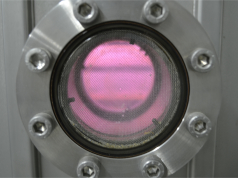
- PECVD reactor. Plasma enhanced chemical vapor deposition of silicon nitride coatings. Up to 4” wafers.
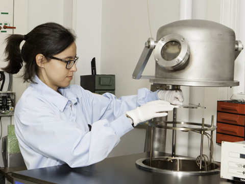
- Photolithography mask aligner for 2’’ wafers
- Physical Vapor Deposition Equipment. E-gun and Joule-effect evaporation. Ti, Pd, Ag, Al. Up to to 4” wafers
|
|
 |
2. Manufacturing of multijunction and advanced solar cells
- Cleaning and etching wet benches: acids, organics, plasma asher, contact layer etching, mesa etching
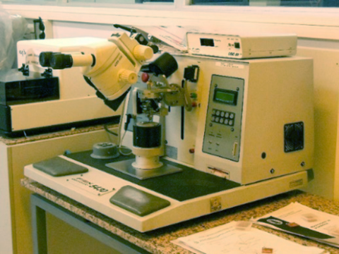
- Photolithography Mask aligner - SUSS MicroTec MJB4. High-resolution photolithography in substrates and wafers up to 4''/ 100mm.
- Wirebonder DELVOTEK 5430. Equipment to make aluminum/gold wire connections with 17.5 to 75 um diameter.
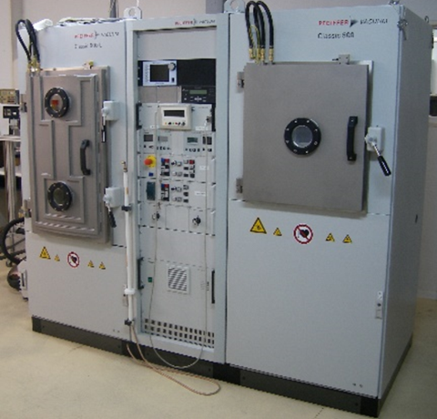
- Electron Beam Physical Vapor Deposition Tool- Classic 500 Twin High Vacuum Coating System. Separate chambers for metal and dielectric coatings
- Joule effect Physical Vapor Deposition Tool for metals- Telstar Vacudel 300
- Joule effect Physical Vapor Deposition tool for dielectrics
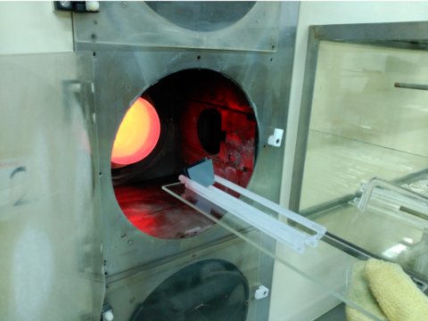
- Rapid Thermal Process (RTP). Wafers up to 6’’; maximum heat slope of 75 K/s and temperatures up to 1000 °C; Anneal atmospheres available: Nitrogen, Hydrogen and Forming.
- Plasma asher. Low pressure plasma system from DIENER ELCTRONIC to clean semiconductor wafers.
- Sputtering system to produce thin films. PVD-MT/2M3T equipped with two sputtering RF magnetrons and three resistive thermal evaporation sources in the same process chamber.
Official rates for these services can be found at UPM WEB SITE. |
|
 |